

 Product
 Brand
Brand Articles
 Tools
Tools
AMD Xilinx vs. Intel Altera FPGA Comparison: Architecture, Toolchains, and Selection Guide
Choosing between AMD Xilinx and Intel Altera FPGAs requires evaluating architectural differences that affect logic density, DSP throughput, and toolchain workflows. For hardware engineers and system architects, the choice between AMD Xilinx and Intel Altera is not merely a component selection—it dictates firmware toolchain workflows, intellectual property (IP) ecosystem compatibility, and long-term supply chain architecture.
AMD Xilinx provides heterogeneous system-on-chip (SoC) architectures, vector-based dedicated AI Engines (AIEs), and standardized AMBA AXI4 interconnects. Altera delivers high core clock frequencies through fine-grained register retiming (HyperFlex), modular transceiver chiplet integration via Embedded Multi-die Interconnect Bridges (EMIB), embedded in-fabric tensor arithmetic, and performant asymmetric Arm processing subsystems in mid-range tiers. This guide evaluates both ecosystems across silicon microarchitecture, digital signal processing (DSP), high-speed serial protocols, software development environments, and migration trade-offs.
Corporate Landscape and Product Portfolio Mapping
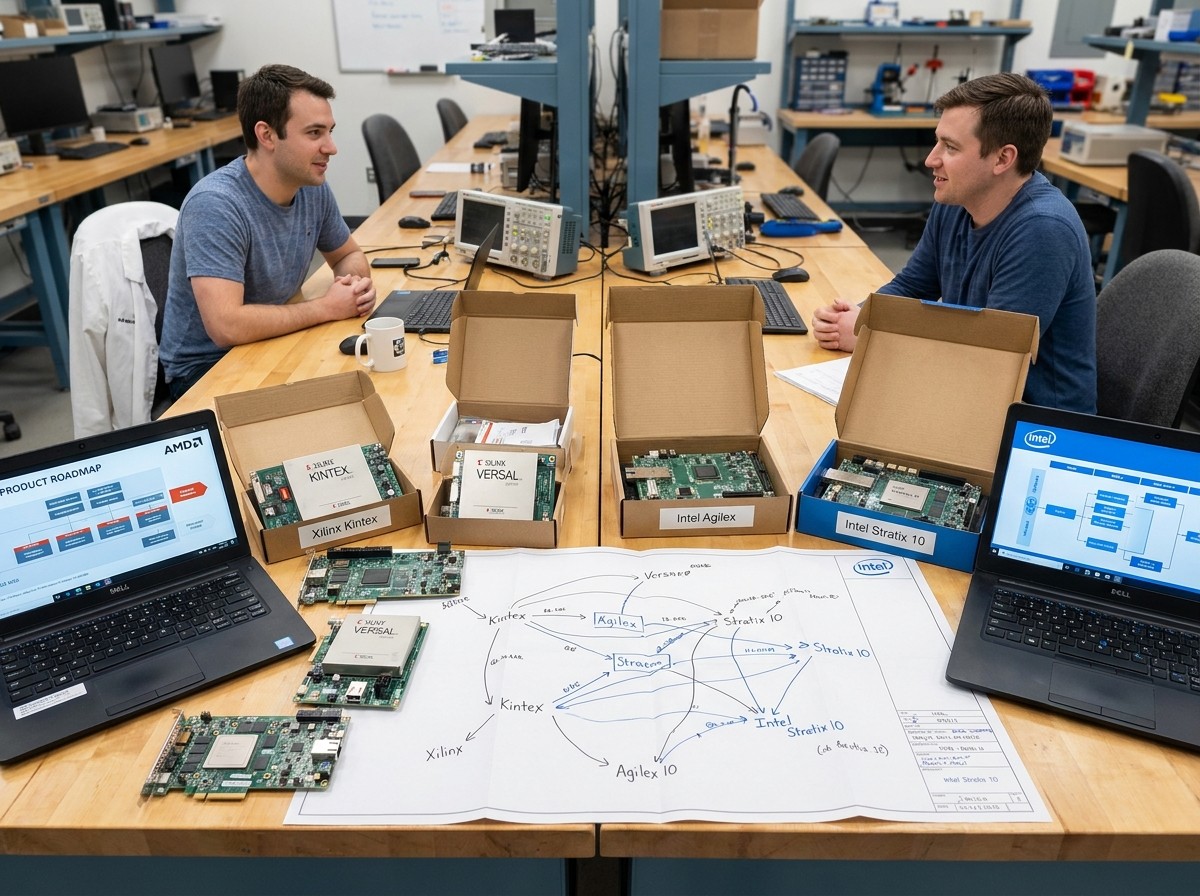
Understanding vendor stability and manufacturing partnerships is essential when committing to long-term aerospace, industrial, defense, or communications deployments. Both vendors have undergone significant structural reorganizations that define their current fabrication strategies and product roadmaps.
AMD completed its acquisition of Xilinx in February 2022, establishing the Adaptive and Embedded Computing Group (AECG). AMD relies primarily on Taiwan Semiconductor Manufacturing Company (TSMC) for silicon fabrication, utilizing TSMC’s 16nm, 7nm, and 5nm/4nm FinFET processes across its UltraScale+ and Versal portfolios.
Altera, originally acquired by Intel in 2015 as the Programmable Solutions Group (PSG), was rebranded back to Altera as an independent business in early 2024. In April 2025, Intel entered into a definitive agreement to sell a 51% controlling stake in Altera to private equity firm Silver Lake at an enterprise valuation of $8.75 billion[3], a transaction that closed in September 2025 with Raghib Hussain serving as Chief Executive Officer. Altera operates as an independent pure-play FPGA provider utilizing both Intel Foundry and external foundry capacity.
Cross-Vendor Device Alignment
To establish parity across application requirements, device families are organized into four distinct tiers:
| Market Tier | AMD Xilinx Portfolio | Altera Portfolio | Primary Architectural Focus |
|---|---|---|---|
| Cost-Optimized / Low-Power | Spartan-7, Artix-7, Artix UltraScale+ | MAX 10, Cyclone 10 LP/GX, Agilex 3 | I/O expansion, board management, low-power edge control |
| Mid-Range Logic & Compute | Kintex-7, Kintex UltraScale+ | Arria 10, Agilex 5 | High DSP density, 25G/50G transceivers, embedded vision |
| High-End & Hyperscale Logic | Virtex UltraScale+, Versal Premium | Stratix 10, Agilex 7, Agilex 9 | 100G–800G networking, high-density logic emulation, radar |
| Heterogeneous Adaptive SoCs | Versal Prime, AI Core, AI Edge | Agilex 5 SoC, Agilex 7 SoC | Hard processor subsystems, dedicated AI acceleration, NoC |
Logic Fabric and Microarchitecture: CLB vs. ALM
The low-level building blocks of AMD and Altera silicon represent fundamentally different approaches to look-up table (LUT) packing density, register allocation, and routing congestion.
Configurable Logic Block (CLB) vs. Adaptive Logic Module (ALM)
AMD fabrics utilize the Configurable Logic Block. In the UltraScale and Versal architectures, each CLB contains multiple 6-input LUTs (LUT6) with two associated flip-flops per LUT, dedicated wide-multiplexer circuitry, and dedicated carry lookahead chains. A single LUT6 can implement any arbitrary 6-input Boolean function or be configured as two 5-input functions that share common inputs.
Altera fabrics rely on the Adaptive Logic Module. An ALM contains an 8-input fracturable LUT that splits into two fully independent smaller LUTs (such as two 4-input, two 5-input, or specific 6-input configurations) without sharing all inputs. An ALM integrates four dedicated registers alongside carry-chain logic. This fracturable arrangement provides higher logic density when synthesizing complex control logic containing diverse input widths.
| Feature | Architectural Distinction |
|---|---|
| Basic Logic Cell | AMD CLB (LUT6 + 2 FFs) vs. Altera ALM (8-LUT + 4 FFs) |
| Routing Registers | Traditional switch matrix vs. HyperFlex Hyper-Registers |
| Primary Routing Bottleneck | Interconnect wire delay vs. Logic-level delay |
| Target Clock Optimization | Deep structural pipelining vs. Compiler register retiming |
Interconnect Routing and HyperFlex Technology
In conventional FPGA architectures, as designs exceed 70% fabric utilization, signal routing delays across programmable interconnect switches surpass logic gate delays. However, AMD and Altera take different approaches to mitigate this bottleneck. AMD addresses this in its UltraScale+ and Versal architectures by deploying segmented routing tracks, distributed clock buffers, and hardened Network-on-Chip (NoC) interconnects to bypass standard fabric routing for system-level traffic.
Altera introduced the HyperFlex Architecture in Stratix 10 and refined it in Agilex. HyperFlex embeds bypassable registers—termed Hyper-Registers—at every routing segment and functional block input throughout the entire fabric core.
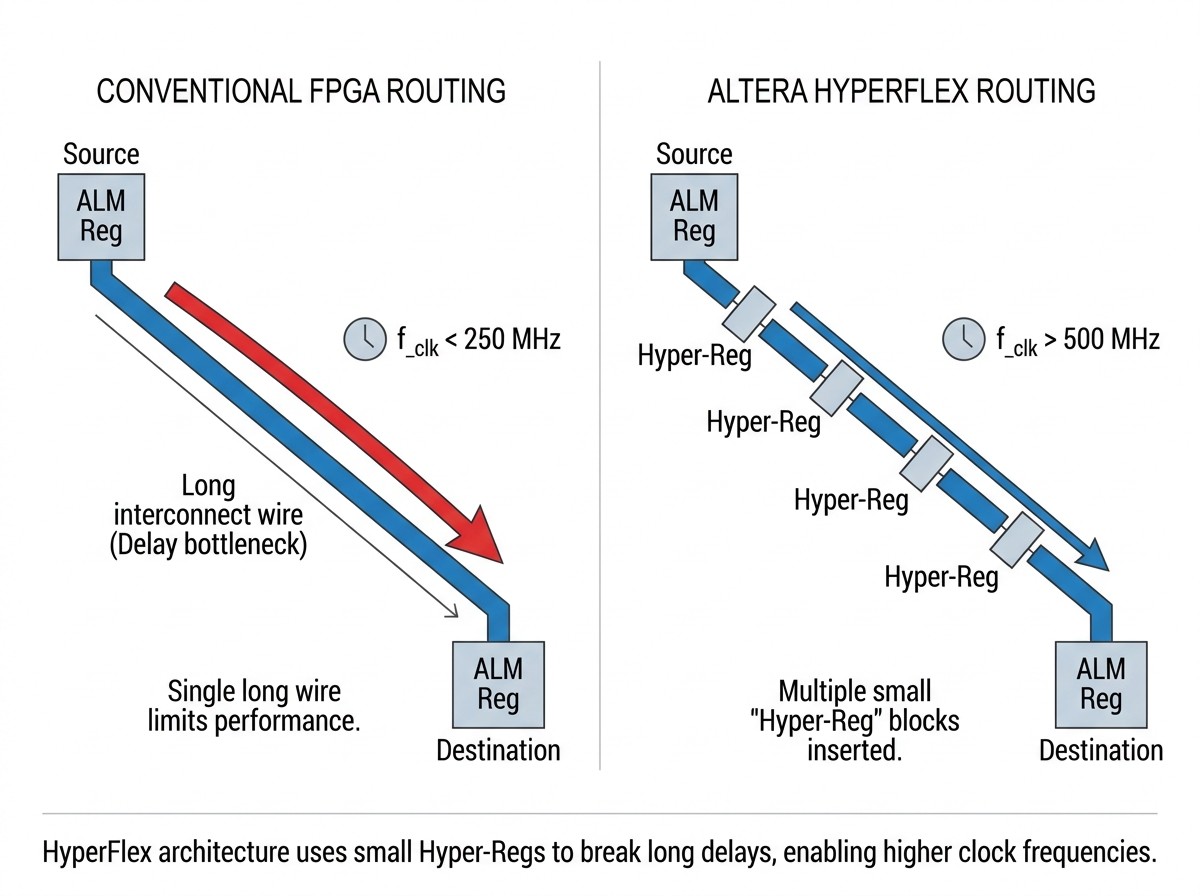
Instead of consuming standard logic-cell registers to break critical paths, the Quartus Prime compiler automatically shifts (retimes) registers into the interconnect network. This eliminates setup and hold time bottlenecks on long routing tracks, enabling Agilex core logic to reach clock frequencies () up to 40% higher than traditional non-retimed fabrics when RTL is written with sufficient pipeline depth.
Counter-Intuitive Engineering Fact: Simply migrating legacy Verilog/VHDL directly to an Altera HyperFlex architecture will not automatically improve. If RTL contains asynchronous resets or unpipelined feedback control loops, the compiler cannot push registers into the routing fabric. Maximizing HyperFlex performance requires synchronous design practices and removing asynchronous clear assertions on data pipelines.
Embedded Memory Hierarchies
On-chip memory distribution determines buffer throughput in digital signal processing and network packet filtering:
AMD Memory Architecture: Distributed LUT RAM (64 bits per LUT), dedicated 36 Kb Block RAM blocks (BRAM, configurable as dual independent 18 Kb primitives), and high-density 288 Kb UltraRAM (URAM) blocks. UltraRAM acts as an on-chip SRAM cache, filling the capacity gap between BRAM and external DDR4/DDR5/HBM.
Altera Memory Architecture: Memory Logic Array Blocks (MLAB, 640 bits per block for shallow FIFO buffers), 20 Kb embedded memory blocks (M20K), and centralized embedded SRAM (eSRAM) macro blocks operating as low-latency, high-bandwidth system buffers in high-end Agilex variants.
DSP Slices and Edge AI Acceleration Microarchitecture
Real-time signal processing and machine learning inference workloads depend heavily on the structure of hard arithmetic blocks.
Arithmetic Primitives: AMD DSP58 vs. Altera AI Tensor Blocks
AMD's flagship Versal architecture deploys the DSP58 slice, a wide arithmetic execution unit that improves upon the legacy DSP48E2 primitive found in UltraScale+ devices:
Features a
-bit two's-complement multiplier.
Integrates a 58-bit accumulator to eliminate overflow during deep accumulation sequences.
Supports native single-precision floating-point operations.
Provides a dedicated three-element vector INT8 dot-product mode (
), processing three parallel 8-bit integer multiplications within a single DSP block cycle.
Altera’s modern portfolio incorporates specialized Variable-Precision DSP with AI Tensor Blocks:
Agilex 5 features an Enhanced DSP block that delivers up to 20 INT8 multiplications per block—a
increase in mathematical density[4] compared to previous-generation Agilex DSP blocks.
High-end Stratix 10 NX variants incorporate AI Tensor Blocks containing 30 INT8 and 60 INT4 dot-product multipliers per block.
Provides native hardware support for FP32, FP16, and Brain Floating Point (Bfloat16) operations, allowing engineers to infer quantized deep neural networks directly inside the fabric without synthesizing soft-logic floating-point conversion units.
Heterogeneous Vector Processors vs. Homogeneous Fabric-Infused AI
The structural divergence between AMD and Altera is most pronounced in their approaches to AI acceleration. Conversely, their packaging strategies also differ significantly:
AMD Versal AI Engines (AIE-ML / AIE-2): AMD utilizes a heterogeneous tiling approach. Dedicated AI Engine tiles reside as an independent, hardened 2D vector array adjacent to the programmable logic. Each AIE tile contains a 512-bit SIMD/VLIW vector processor, dedicated local SRAM, and autonomous DMA controllers interconnected by a memory-mapped streaming network. The programmable logic handles I/O aggregation and pre-processing, while vector calculations are offloaded via the Network-on-Chip (NoC).
Altera Homogeneous Fabric-Infused AI: Altera embeds AI Tensor Blocks uniformly throughout the general FPGA routing fabric. This allows developers to build arbitrary systolic arrays and custom tensor datapaths directly inside the logic grid, eliminating the latency of routing data across an offload boundary into a distinct compute tile.
Packaging, High-Speed Transceivers, and Interconnect Protocols
Modern high-bandwidth applications require advanced multichip module (MCM) packaging to interface high-speed serial links with core logic.
Interposer Integration vs. Chiplet Tiles
AMD employs Stacked Silicon Interconnect (SSI) technology for large-scale devices. High-density FPGAs are partitioned into multiple Super Logic Regions (SLRs) fabricated on standard processes and mounted side-by-side onto a passive silicon interposer containing dense micro-bumps. While SSI enables monolithic-like logic scaling across large footprints, crossing an SLR boundary via inter-die routing introduces measurable clock and routing skew that Static Timing Analysis (STA) engines must constrain.
Altera utilizes Intel’s Embedded Multi-die Interconnect Bridge (EMIB) technology. Instead of a large, costly silicon interposer spanning the entire package base, EMIB embeds ultra-dense silicon bridges locally within an organic substrate. This links the central FPGA logic die to modular, heterogeneous transceiver and protocol chiplets (such as F-Tiles and R-Tiles). This chiplet strategy enables Altera to rapidly update transceiver standards without re-spinning the central logic fabric[3].
Serializer/Deserializer (SerDes) and Protocol Hardening
The physical transceiver capabilities and hardened interface stacks differ across both flagship platforms:
| Specification | AMD Versal Portfolio | Altera Agilex 7 Portfolio |
|---|---|---|
| Maximum SerDes Speed | 112 Gbps PAM4 (GTM) | 116 Gbps PAM4 (F-Tile) |
| Mid-Tier SerDes Speed | 32 Gbps NRZ / 58G PAM4 | 58 Gbps PAM4 / 32G NRZ (F-Tile) |
| Packaging Method | SSI Passive Interposer | Localized EMIB Chiplet Bridges |
| Protocol Hard IP | PCIe Gen 5, CXL 2.0 CPM | PCIe Gen 5, CXL 1.1/2.0 R-Tile |
| Die-to-Die Skew Risk | Inter-SLR Crossing Skew | Interface Bridge Latency |
AMD Versal deployments integrate GTYP transceivers (up to 32 Gbps NRZ and 58 Gbps PAM4) for standard backplane connectivity and GTM transceivers (reaching 112 Gbps PAM4) for high-performance 800G optical networking. Protocol hardening includes integrated PCIe Gen 5 and Compute Express Link (CXL 2.0) via the Core Processing and Memory (CPM5/CPM6) hard block.
Altera Agilex 7 couples its core fabric to F-Tile transceivers (supporting data rates up to 116 Gbps PAM4 and 58 Gbps NRZ) alongside R-Tile chiplets, which feature hardened PCIe Gen 5 and CXL 1.1/2.0 protocol stacks. The modular nature of EMIB gives Altera flexibility in configuring custom multi-tile combinations for specialized radar and data center appliances.
Embedded Processor Subsystems and Soft-Core Evolution
The integration of hardened microprocessor cores (SoC FPGAs) allows single-chip platforms to execute Linux operating systems, safety-critical real-time loops, and reconfigurable digital logic concurrently.
Hard Processor Subsystems: AMD CIPS vs. Altera HPS
AMD SoC Architecture: The legacy Zynq UltraScale+ family integrates a processing subsystem featuring quad Arm Cortex-A53 application cores, dual Cortex-R5F real-time cores, and a Mali-400 GPU. Modern Versal devices utilize the Control, Interfaces, and Processing System (CIPS), featuring dual Cortex-A72 cores (transitioning to quad Cortex-A78AE safety cores in Versal Gen 2) coupled with dual Cortex-R5F/R52 real-time processors and a dedicated Platform Management Controller (PMC).
Altera SoC Architecture: While high-end Agilex 7 devices utilize quad Cortex-A53 cores, Altera implemented an asymmetric Arm architecture in its mid-range Agilex 5 platform. Agilex 5 integrates a hard processor subsystem (HPS) combining two high-performance Cortex-A76 cores with two power-efficient Cortex-A55 cores in an Arm DynamIQ configuration, providing superior embedded Linux processing power compared to legacy mid-range FPGAs.
Industry Convergence on RISC-V Soft Cores
For applications requiring soft processor cores synthesized within the general FPGA fabric, both vendors have deprecated their legacy proprietary 32-bit architectures in favor of open-standard RISC-V implementations:
AMD has transitioned from its proprietary MicroBlaze architecture to MicroBlaze V, a soft-core processor implementing the standard 32-bit (RV32) and 64-bit (RV64) RISC-V instruction set.
Altera has retired the Nios II processor in favor of Nios V, built upon the RV32I/E RISC-V core specification[8].
This migration allows engineering teams to standardize their compiler toolchains around upstream GCC and LLVM, eliminating vendor-locked IDEs and proprietary RTOS board support packages.
Development Toolchains, Compilation Mechanics, and Licensing
The development software ecosystem dictates engineering iteration speed, place-and-route determinism, timing closure feasibility, and annual operating costs.
Vivado Design Suite vs. Quartus Prime Pro
Timing Closure and Compilation: AMD’s Vivado Design Suite is recognized for its unified data model and deterministic Static Timing Analysis (STA). Vivado allows comprehensive intra-clock and inter-clock timing adjustments directly through standard Synopsys Design Constraints (SDC) translated into Xilinx Design Constraints (XDC). Altera’s Quartus Prime Pro Edition features a compiler optimized for register retiming across HyperFlex routing tracks. While Quartus Prime Pro handles high-density designs well, designs pushing fabric limits often require multi-seed exploration passes (
DSE - Design Space Explorer) to achieve timing closure across high-fanout nets.System-Level IP Integration: AMD provides Vivado IP Integrator (IPI), a graphical and scriptable design canvas standardized natively on the AMBA AXI4 protocol. Connecting high-speed streaming or memory-mapped IP blocks is streamlined due to native bus automation. Altera provides Platform Designer (formerly Qsys), which natively handles both Avalon-MM/Avalon-ST and AMBA AXI interfaces. Platform Designer uses automatic interconnect generation and clock-domain crossing bridges, which simplifies mixed-protocol systems but can introduce logic overhead if interconnect switches are improperly parameterized.
High-Level Synthesis (HLS): AMD Vitis HLS allows developers to compile C/C++ algorithms directly into synthesizable RTL, integrated with the Vitis AI execution environment. Altera leverages the Intel oneAPI toolkit and the FPGA AI Suite, targeting OpenCL and SYCL heterogeneous programming paradigms.
| Attribute | AMD Vivado ML | Altera Quartus Prime Pro |
|---|---|---|
| Primary IP Bus | AMBA AXI4 Native | Avalon-MM / AXI Bridges |
| Timing Constraints | XDC (SDC-based) | SDC Native |
| HLS Environment | Vitis Unified IDE (C/C++) | oneAPI / FPGA AI (SYCL) |
| Full Desktop Disk Size | ~62 GB (17.3 GB download) | ~55 GB (Modular installer) |
| Free Version Longevity | Basic Tier (Annual Renewal) | Lite Edition (Perpetual) |
| Free Device Support | 7 Series, Low UltraScale+ | MAX, Cyclone Families |
Licensing Tiers, Storage Footprints, and Operational Overhead
Software environments require substantial IT storage, compute resources, and annual license tracking:
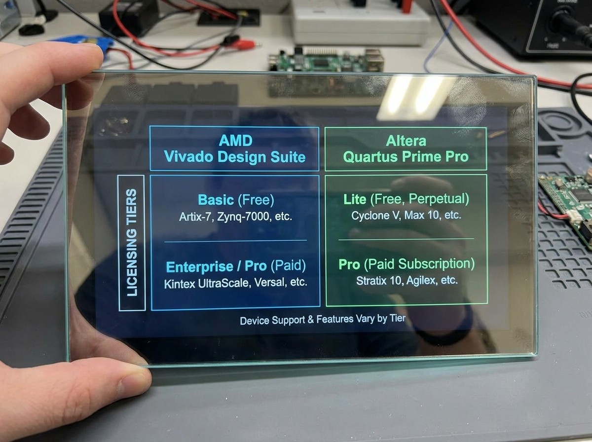
Toolchain installation profiling shows that a standard desktop installation of AMD Vivado Design Suite occupies ~62 GB of local disk space, extracted from a 17.33 GB compressed download payload. AMD has restructured its software licensing into distinct tiers: Basic, Core, Pro, Enterprise, and Gold. The free Basic Tier has replaced the legacy WebPACK model.
Critical Licensing Note: The free Vivado Basic Tier requires an active node-locked license bound to the host system. When configuring this in the AMD Product Licensing portal, engineers must extract system parameters (
Host Name,Disk Drive Serial Number, orEthernet MAC ID) directly from the Vivado License Manager. Furthermore, the free Basic license carries a strict one-year expiration limit, requiring developers to re-generate and bind a fresh license file annually. Launching modern Vivado without a pre-bound license generates an immediate execution failure popup.
Altera splits its software into three tiers: Quartus Prime Lite Edition (perpetual, free, requires no license file, supporting MAX and Cyclone devices), Standard Edition (legacy mid-range Arria/Cyclone devices), and Pro Edition (paid annual seat subscription, mandatory for Agilex and Stratix 10 families).
Pro Tip for Storage-Constrained Workstations: When provisioning build environments or continuous integration (CI/CD) synthesis runners, engineers can prevent disk bloat by deselecting unneeded device families during installation. Installing only specific target parts (or bare Engineering Sample devices) reduces the Vivado or Quartus footprint on local storage by up to 60%.
Migration Obstacles, Vendor Lock-in, and Hardware Portability
Migrating an established FPGA design between AMD Xilinx and Altera architectures involves far more than recompiling Verilog or VHDL source files. Hardware engineers must account for proprietary primitives, clock routing architectures, memory latency differences, and PCB package layouts.
Clock Buffering and Global Tree Conversion
Clock topologies cannot be directly cross-compiled due to proprietary clock multiplexing and regional buffer primitives:
AMD designs rely heavily on
BUFG,BUFGCE,BUFG_GT(for transceivers), andIBUFDSdifferential input buffers.Altera architectures require instantiation of
ALTCLKCTRLor specialized regional clock distribution primitives (clkctrl). Clock routing networks must be structurally refactored in the RTL to ensure clock enable pins map to physical routing tracks correctly without introducing hold-time violations.
Memory Primitive Mapping and Pipeline Delays
While small distributed RAMs (LUT RAM vs. MLAB) infer cleanly from standard HDL templates, deep Block RAMs present subtle migration issues:
AMD UltraRAM operates as a fixed 288 Kb synchronous block with defined single-cycle or multi-cycle output register pipeline modes.
Altera M20K blocks (20 Kb) have distinct timing models and address-to-data output latency behaviors. If RTL assumes an implicit two-cycle pipeline structure specific to AMD BRAM or UltraRAM, synthesizing onto Altera M20K blocks will produce read/write hazard mismatches unless read-enable and output-register stages are re-architected.
High-Speed Transceiver Wrappers and Protocol Adapters
Physical layer transceivers cannot be ported across vendors:
AMD transceiver configurations are generated through the Vivado Transceiver Wizard, which wraps low-level primitives (
GTYE4_COMMON,GTHE4_CHANNEL,GTM).Altera requires generating fresh Native PHY IP cores configured specifically for the target architecture's F-Tile or E-Tile transceivers.
System architects must isolate transceiver wrappers behind abstract FIFO/gearbox boundary interfaces in RTL, preventing vendor-specific SerDes configuration registers from leaking into the core application logic.
Board-Level Electrical and Pinout Incompatibilities
Dual-sourcing a single PCB layout between AMD and Altera is virtually impossible:
BGA Pin Mapping: Ball grid array (BGA) package pinouts are entirely incompatible. Power, ground, transceiver high-speed TX/RX pairs, and bank I/O assignments do not align across vendor package footprints.
Power Rail Sequencing: Power delivery networks (PDN) require distinct voltage rails and strict power-up slew-rate sequencing. AMD Versal requires specific core voltage tracking (
) and processing subsystem sequencing (
), while Altera Agilex requires unique smart voltage ID (SmartVID) digital PWM regulation to manage multi-die EMIB tile loads dynamically.
Architect's Selection Matrix and Evaluation Framework
To evaluate platform selection across technical, commercial, and architectural criteria, consult the decision matrix below:
| Architectural Dimension | AMD Xilinx Portfolio | Intel / Altera Portfolio | Strategic Winner / Fit |
|---|---|---|---|
| Core Flagship Family | Versal Adaptive SoC (ACAP) | Agilex 7 / Agilex 9 / Agilex 5 | Context-dependent |
| Logic Cell Architecture | Configurable Logic Block (LUT6) | Adaptive Logic Module (Fracturable 8-LUT) | Altera for pure logic packing density |
| Interconnect Routing | Monolithic & SLR Interconnects | HyperFlex 2 (Pervasive Hyper-Registers) | Altera for highregister retiming |
| Embedded DSP | DSP58 (, 58-bit Accumulator) | Variable-Precision DSP (, FP32/16) | AMD for wide integer dot-products |
| AI Acceleration Model | Dedicated 2D Vector Tile Mesh (AIE-ML) | In-Fabric AI Tensor Blocks | AMD for vector offload; Altera for systolic arrays |
| Advanced Packaging | Stacked Silicon Interconnect (SLR) | Modular EMIB Chiplet Bridges | Altera for modular transceiver customization |
| Max Transceiver Speed | 112 Gbps PAM4 (GTM SerDes) | 116 Gbps PAM4 (F-Tile SerDes) | Altera for maximum raw SerDes line rate |
| Mid-Range SoC Processing | Zynq UltraScale+ (Quad Cortex-A53) | Agilex 5 (Dual Cortex-A76 + Dual A55) | Altera for application processor compute |
| Safety-Critical SoC | Versal Gen 2 (Cortex-A78AE / R52) | Agilex 7 SoC (Cortex-A53) | AMD for ASIL-D automotive/safety domains |
| Soft-Core Processor | MicroBlaze V (Open RISC-V) | Nios V (Open RISC-V) | Tie (Both support open RISC-V standards) |
| IP Bus Architecture | Native AMBA AXI4 | Avalon-MM / AXI Interconnect Bridges | AMD for standardized AXI ecosystems |
| Free Software Tier | Vivado Basic (Annual Node-Locked Reg.) | Quartus Prime Lite (Perpetual, No Key) | Altera for friction-free legacy use |
Practical Checklist and Implementation Strategy
Hardware engineers and system architects should execute the following technical evaluation steps prior to schematic capture and layout commitment:
Synthesize Representative RTL Modules: Extract timing-critical pipelines from your application (such as FFT filters, packet parsers, or matrix multipliers) and synthesize them concurrently in both Vivado ML Enterprise and
References
AMD Design Conversion for Altera FPGAs and SoCs Methodology Guide (UG1192) — Advanced Micro Devices, Inc. (AMD)
Versal Adaptive SoC Technical Reference Manual (AM011) — Advanced Micro Devices, Inc. (AMD)
Agilex 7 FPGAs and SoCs Device Overview — Altera Corporation / Intel Corporation
Agilex 5 FPGAs and SoCs Device Overview — Altera Corporation / Intel Corporation
Intel Agilex Variable Precision DSP Blocks User Guide — Intel Corporation / Altera Corporation
Versal Architecture and Product Data Sheet: Overview (DS950) — Advanced Micro Devices, Inc. (AMD)
Zynq UltraScale+ MPSoC Data Sheet: Overview (DS891) — Advanced Micro Devices, Inc. (AMD)
Nios V Processor Reference Manual — Altera Corporation / Intel Corporation
 UTMEL
UTMEL
We are the professional distributor of electronic components, providing a large variety of products to save you a lot of time, effort, and cost with our efficient self-customized service. careful order preparation fast delivery service
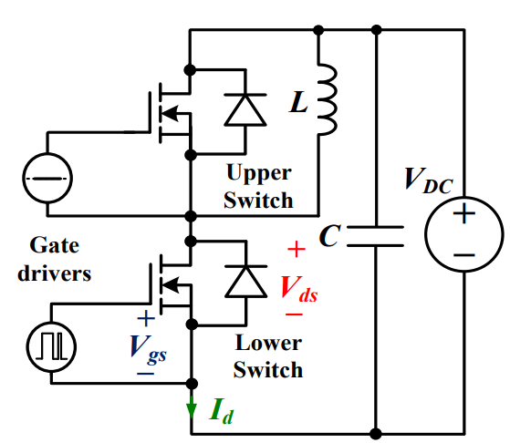 Discovering New and Advanced Methodology for Determining the Dynamic Characterization of Wide Bandgap DevicesSaumitra Jagdale15 March 20242886
For a long era, silicon has stood out as the primary material for fabricating electronic devices due to its affordability, moderate efficiency, and performance capabilities. Despite its widespread use, silicon faces several limitations that render it unsuitable for applications involving high power and elevated temperatures. As technological advancements continue and the industry demands enhanced efficiency from devices, these limitations become increasingly vivid. In the quest for electronic devices that are more potent, efficient, and compact, wide bandgap materials are emerging as a dominant player. Their superiority over silicon in crucial aspects such as efficiency, higher junction temperatures, power density, thinner drift regions, and faster switching speeds positions them as the preferred materials for the future of power electronics.
Read More Applications of FPGAs in Artificial Intelligence: A Comprehensive GuideUTMEL29 August 20255613
This comprehensive guide explores FPGAs as powerful AI accelerators that offer distinct advantages over traditional GPUs and CPUs. FPGAs provide reconfigurable hardware that can be customized for specific AI workloads, delivering superior energy efficiency, ultra-low latency, and deterministic performance—particularly valuable for edge AI applications. While GPUs excel at parallel processing for training, FPGAs shine in inference tasks through their adaptability and power optimization. The document covers practical implementation challenges, including development complexity and resource constraints, while highlighting solutions like High-Level Synthesis tools and vendor-specific AI development suites from Intel and AMD/Xilinx. Real-world applications span telecommunications, healthcare, autonomous vehicles, and financial services, demonstrating FPGAs' versatility in mission-critical systems requiring real-time processing and minimal power consumption.
Read More The 2026 Engineer’s Guide: Choosing the Right MCU for Your Next IoT & New Energy ProjectUTMEL30 April 20261913
A comprehensive comparison of 2026's leading MCUs from ST, NXP, and Microchip across power efficiency, processing performance, connectivity, and ecosystems to help engineers select the optimal chip for next-gen IoT and new energy projects.
Read More AI Server Components: Engineering Next-Gen Data Center Hardware for 100kW RacksUTMEL15 May 20261019
The transition from traditional enterprise IT to AI-driven workloads has rendered legacy data center hardware obsolete, forcing infrastructure planners to re-engineer server components for extreme thermal environments.
Read More The Practical Engineer’s Guide to the NE555N Timer: Pinout, Setup, and TroubleshootingUTMEL29 May 2026823
This comprehensive guide explores the NE555N timer, detailing its 8-pin layout, internal architecture, and key datasheet specifications. It compares the bipolar IC to CMOS variants and details setup configurations for astable, monostable, and bistable modes. Additionally, the guide offers practical troubleshooting advice to prevent common breadboard failures, such as floating reset pins and electrical noise issues.
Read More
Subscribe to Utmel !
![MOC3061SR2VM]() MOC3061SR2VM
MOC3061SR2VMON Semiconductor
![MOC3061SVM]() MOC3061SVM
MOC3061SVMON Semiconductor
![ATECC608A-SSHCZ-T]() ATECC608A-SSHCZ-T
ATECC608A-SSHCZ-TMicrochip Technology
![FOD420S]() FOD420S
FOD420SON Semiconductor
![DLPA1000YFFT]() DLPA1000YFFT
DLPA1000YFFTTexas Instruments
![HCS201/P]() HCS201/P
HCS201/PMicrochip Technology
![AT88SC0404CA-TH]() AT88SC0404CA-TH
AT88SC0404CA-THMicrochip Technology
![DLPC300ZVB]() DLPC300ZVB
DLPC300ZVBTexas Instruments
![FOD4118SV]() FOD4118SV
FOD4118SVON Semiconductor
![MOC3051VM]() MOC3051VM
MOC3051VMON Semiconductor


